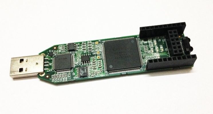
A word before we proceed: If you haven't already had a look at my previous note introducing the open source tool-chain and deployment of basic blinky circuit on FPGA, I recommend reading that before you proceed further. This note assumes you read through the previous one and talks about what might the internals of the FPGA look like. Read it here -
Making an AND Gate
Let's talk about a simple two input AND gate. It takes two inputs, say A and B and has an output C. We will refer to positive logic as we talk so we avoid confusion. What that means is a 1 represents digital HIGH and a 0 a digital LOW. So
AND 1 only if both its inputs are 1
That's the definition of AND gate. Now, think about how it may be implemented?
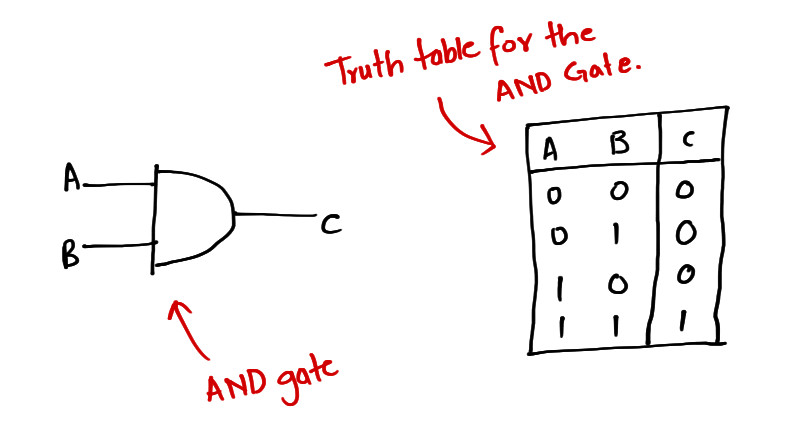
Well one way is to go down at the semiconductor physics level and arrange transistors to make an AND gate. The problem with this is you need lot of industrial equipment/process, special technologies, experienced labour, time etc etc. That's too much of work for a single AND gate. If you were to design a digital circuit full of gates and go build them by putting one transistor at a time, you know you'd be planning to suicide. But what else can be done? The AND gate's working is represented by its truth table. In fact,
truth table
So, if we can cook up
a machine that can look at the inputs, read through the table and tell us what the output has to be,
we would have found a way to implement a gate. Of Course this comes at a cost of a circuit that is generic, power hungry and bulky. Meaning that it takes more number of transistors to make it than just the AND gate, but it's easy to make, so saves a lot of time. Some manufacturer could give us a chip with sea of transistors and we could connect connections between these transistors and make the machine. Since this machine reads through a table, it can be used to implement almost any digital circuit. After all it's just looking at the input, then looking up the answer in a table and telling the output. The Manufacturer could in fact make lot of these machines on a single chip and sell that instead ( this is what Xilinx and Intel does roughly :) ). We could program the machine to behave like different digital circuits based on the truth table it is trying to look up. Implementing a digital circuit is thus, putting it's truth table in the chip. Easy and powerful eh?
This in fact is the central idea of FPGAs. The machine that does the job of reading through table to see what the output has to be for the given inputs is called a LUT a.k.a Lookup Table. Yes! The name is very obvious and so is the functionality. This is the key component/machine of an FPGA and everything else that lives inside it is just a supporting component. So, Lets make a LUT. The most basic possible one.
LUT - Lookup Table
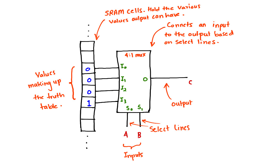
Look at the sketch above and things should start to make sense already if you are trying to guess how a LUT might look. What should be obvious is the "Lookup" part is done using a Multiplexer. Recall that the multiplexer has many inputs, select lines and a single output.
Based on the status of the select lines (S0-S1) it chooses one of the inputs (I0-I3) and connects it to the output (O). So in the sketch below A = 1 and B = 0 (these are the select lines), it reads the memory cell connected to the mux input I2 which happens to be a 0 and connects that to the output and C. C is thus 0. The path is highlighted in Purple.
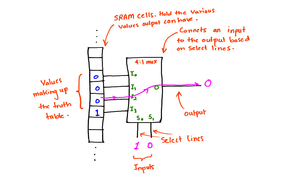
That's all there is to it. The entire hocus-pocus around FPGAs is just the fact that it implements a LUT which is generic and can be used to implement a digital circuit. The inputs of this LUT comes from the memory the select lines from memory and somewhere else (we'll save discussion on that for later :) ). The memory (in this case the SRAM) cells hold the value corresponding to the various output that circuit can have. The two input AND gate can have four different values (All the values in the truth table). Again, the LUT is looking for the value to be output from the memory! Thus, if A = 0, B = 0 then C = I0 (0); if A = 0, B = 1 then C = I1 (0); if A = 1, B = 0 then C = I2 (0) and if A = 1, B = 1 then C = I3 (1). In effect the picture above is seeming to behave like an AND gate!
Do you see how do we put those 0s and 1s in the memory cells? Well, that's the content of the .bin file we flash on the FPGA. The .bin file is a stream of 0s and 1s that just go and sit in the memory. The FPGA interprets these values and automagically realizes the circuit. A part of which involves our hero - "The LUT"! What this magic is we'll discover in the notes to come.
I have to leave you here. I am assuming that the picture of LUT above delights you and gives you intellectual pleasure. While you enjoy that please remember that this is only the most simplest model. There are lot of other questions that we need to address. For instance:
- where do the physical inputs come from?
- Where does the output goto? What happens when the circuit is more complex?
- What about sequential circuits? The signal timings?
Things do get little more involved but the basic idea remains the same, we shall discover those in next note. Until then, cherish the intellectual pleasure :).